(Peer-Reviewed) Broadband high-efficiency dielectric metalenses based on quasi-continuous nanostrips
Xiaohu Zhang 张晓虎 ¹, Qinmiao Chen 陈钦杪 ², Dongliang Tang 汤东亮 ³, Kaifeng Liu 刘开峰 ¹, Haimo Zhang 张海漠 ¹, Lintong Shi 施林彤 ¹, Mengyao He 贺梦瑶 ¹, Yongcai Guo 郭永彩 ¹, Shumin Xiao 肖淑敏 ²
¹ Key laboratory of optoelectronic Technology and Systems of the Education Ministry of China, Chongqing University, Chongqing 400044, China
中国 重庆 重庆大学光电技术及系统教育部重点实验室
² Ministry of Industry and Information Technology Key Lab of Micro-Nano Optoelectronic Information System, Guangdong Provincial Key Laboratory of Semiconductor Optoelectronic Materials and Intelligent Photonic Systems, Harbin Institute of Technology, Shenzhen 518055, China
中国 深圳 哈尔滨工业大学 广东省半导体光电材料与智能光子系统重点实验室 微纳光电信息系统理论与技术工信部重点实验室
³ Key Laboratory for Micro/Nano Optoelectronic Devices of Ministry of Education & Hunan Provincial Key Laboratory of Low-Dimensional Structural Physics and Devices, School of Physics and Electronics, Hunan University, Changsha 410082, China
中国 长沙 湖南大学物理与微电子科学学院 低维结构物理与器件湖南省重点实验室 微纳光电器件及应用教育部重点实验室
Opto-Electronic Advances, 2024-01-31
Abstract
Benefiting from the abrupt phase changes within subwavelength thicknesses, metasurfaces have been widely applied for lightweight and compact optical systems. Simultaneous broadband and high-efficiency characteristics are highly attractive for the practical implementation of metasurfaces. However, current metasurface devices mostly adopt discrete micro/nano structures, which rarely realize both merits simultaneously.
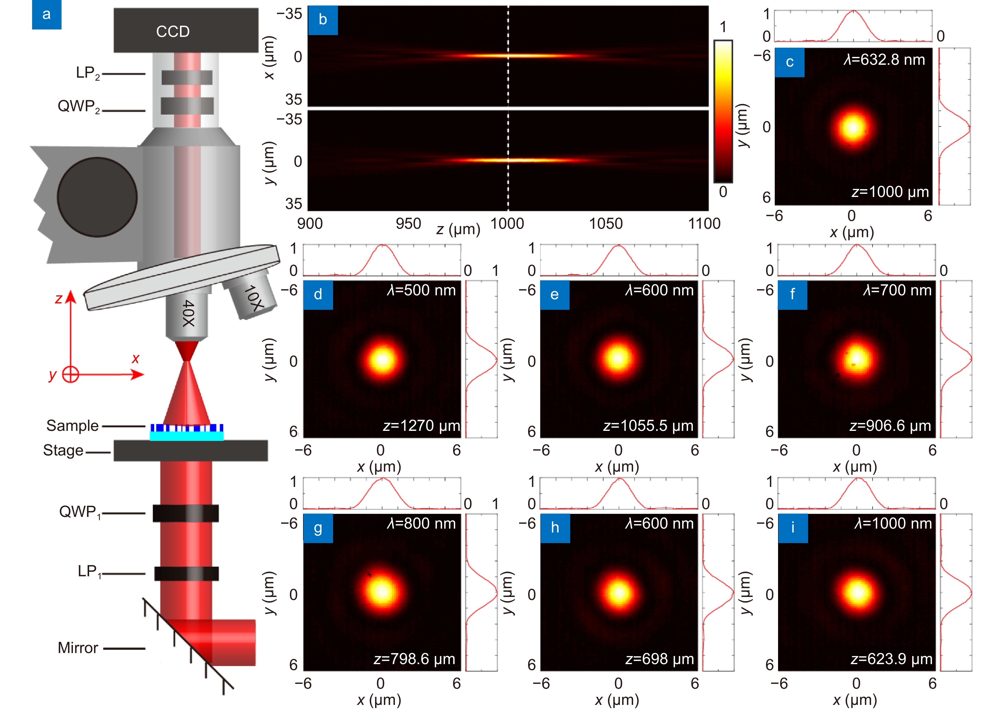
In this paper, dielectric metasurfaces composed of quasi-continuous nanostrips are proposed to overcome this limitation. Via quasi-continuous nanostrips metasurface, a normal focusing metalens and a superoscillatory lens overcoming the diffraction limit are designed and experimentally demonstrated. The quasi-continuous metadevices can operate in a broadband wavelength ranging from 450 nm to 1000 nm and keep a high power efficiency.
The average efficiency of the fabricated metalens reaches 54.24%, showing a significant improvement compared to the previously reported metalenses with the same thickness. The proposed methodology can be easily extended to design other metadevices with the advantages of broadband and high-efficiency in practical optical systems.
Flicker minimization in power-saving displays enabled by measurement of difference in flexoelectric coefficients and displacement-current in positive dielectric anisotropy liquid crystals
Junho Jung, HaYoung Jung, GyuRi Choi, HanByeol Park, Sun-Mi Park, Ki-Sun Kwon, Heui-Seok Jin, Dong-Jin Lee, Hoon Jeong, JeongKi Park, Byeong Koo Kim, Seung Hee Lee, MinSu Kim
Opto-Electronic Advances
2025-09-25
Dual-frequency angular-multiplexed fringe projection profilometry with deep learning: breaking hardware limits for ultra-high-speed 3D imaging
Wenwu Chen, Yifan Liu, Shijie Feng, Wei Yin, Jiaming Qian, Yixuan Li, Hang Zhang, Maciej Trusiak, Malgorzata Kujawinska, Qian Chen, Chao Zuo
Opto-Electronic Advances
2025-09-25
