(Peer-Reviewed) On-chip light control of semiconductor optoelectronic devices using integrated metasurfaces
Cheng-Long Zheng 郑程龙 ¹, Pei-Nan Ni 倪佩楠 ¹, Yi-Yang Xie 解意洋 ², Patrice Genevet ³
¹ Henan Key Laboratory of Diamond Optoelectronic Materials and Devices, Key Laboratory of Materials Physics, Ministry of Education, School of Physics, Zhengzhou University, Zhengzhou 450052, China
中国 郑州 郑州大学物理学院 材料物理教育部重点实验室 河南省金刚石光电材料与器件重点实验室
² Key Laboratory of Optoelectronics Technology, Beijing University of Technology, Ministry of Education, Beijing 100124, China
中国 北京 北京工业大学光电子技术教育部重点实验室
³ Colorado School of Mines, 1523 Illinois St., Golden, CO 80401, USA
Opto-Electronic Advances, 2025-01-07
Abstract
Semiconductor optoelectronics devices, capable of converting electrical power into light or conversely light into electrical power in a compact and highly efficient manner represent one of the most advanced technologies ever developed, which has profoundly reshaped the modern life with a wide range of applications. In recent decades, semiconductor technology has rapidly evolved from first-generation narrow bandgap materials (Si, Ge) to the latest fourth-generation ultra-wide bandgap semiconductor (GaO, diamond, AlN) with enhanced performance to meet growing demands.
Additionally, merging semiconductor devices with other techniques, such as computer assisted design, state-of-the-art micro/nano fabrications, novel epitaxial growth, have significantly accelerated the development of semiconductor optoelectronics devices. Among them, integrating metasurfaces with semiconductor optoelectronic devices have opened new frontiers for on-chip control of their electromagnetic response, providing access to previously inaccessible degrees of freedom.
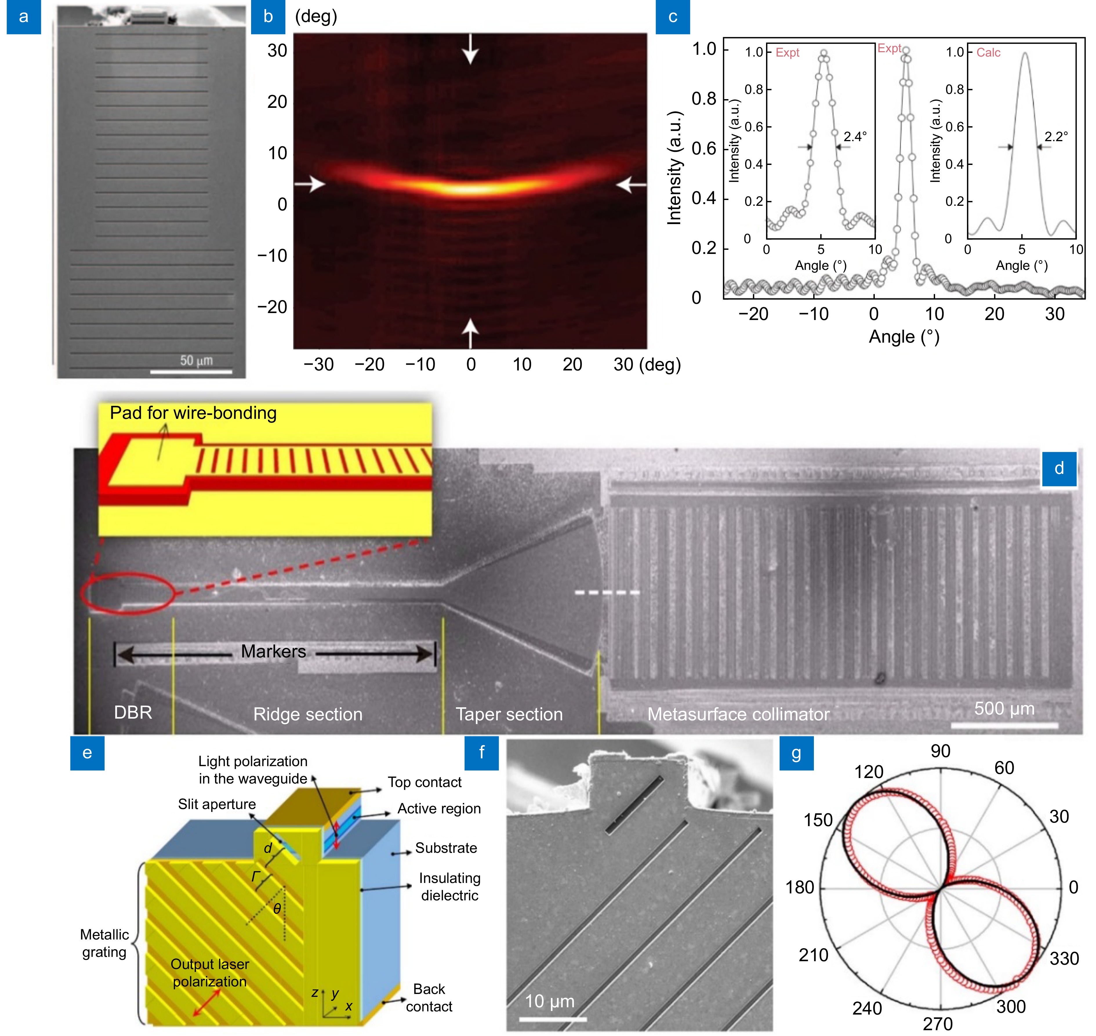
We review the recent advances in on-chip control of a variety of semiconductor optoelectronic devices using integrated metasurfaces, including semiconductor lasers, semiconductor light emitting devices, semiconductor photodetectors, and low dimensional semiconductors. The integration of metasurfaces with semiconductors offers wafer-level ultracompact solutions for manipulating the functionalities of semiconductor devices, while also providing a practical platform for implementing cutting-edge metasurface technology in real-world applications.
High-resolution tumor marker detection based on microwave photonics demodulated dual wavelength fiber laser sensor
Jie Hu, Weihao Lin, Liyang Shao, Chenlong Xue, Fang Zhao, Dongrui Xiao, Yang Ran, Yue Meng, Panpan He, Zhiguang Yu, Jinna Chen, Perry Ping Shum
Opto-Electronic Advances
2024-12-16
Ultra-high-Q photonic crystal nanobeam cavity for etchless lithium niobate on insulator (LNOI) platform
Zhi Jiang, Cizhe Fang, Xu Ran, Yu Gao, Ruiqing Wang, Jianguo Wang, Danyang Yao, Xuetao Gan, Yan Liu, Yue Hao, Genquan Han
Opto-Electronic Advances
2024-10-31
